At the Heart of Virtually Any Computerized Technology
Everything about the low, off white building at the corner of Columbia and Colorado seems to directly contradict the Silicon-Valley-tech-company stereotype, at least at first glance. There are no floor to ceiling glass walls, CEOs in sneakers or video games in the office, although the lawn is admittedly manicured.
However, considering its history, it’s almost no surprise that the company that would eventually be purchased to become the Bend division of Microsemi Corporation should eschew these expectations. In fact, it was another Silicon Valley trope, the fear of corporate espionage, that drove what was then called Advanced Power Technology (APT) to Bend in the first place.
In 1985, the founders of Advanced Power Technology had an idea: a new way to build a high powered transistor. According to Marc Vandenberg, vice president and general manager of the Bend division, they also had a problem: their new method “was so special,” that some other Silicon Valley company was liable to steal it. Thus, a discreet Central Oregon destination became the headquarters where the company would grow to have a staff of over 100 before a successful acquisition by Microsemi in 2006.
It’s an understatement to say that, at least to the layman, the ins and outs of what Microsemi does are a little dry. You could venture hours down an internet rabbit hole trying to understand the product names, from mixed signal integrated circuits to high power transistors, and still not understand the difference between P-type and N-type silicon (hint: google it). However, this inherent verbosity is simply a barrier to entry into a world that is undeniably cool.
To understand exactly what Microsemi-Bend does, one must realize that microprocessor chips (bear with me here) are at the heart of virtually any computerized technology, from key-fobs to ballistic missiles to the cell phone in your pocket. These chips contain transistors which act as switches to control electrical currents. The chips themselves are made of silicon and begin their lives as parts of larger wafers. These wafers originate here in Bend.
The concept is more complicated than it sounds, and after just a few moments in the wafer fabrication building it’s easy to forget that a quarter of an hour ago you didn’t know what silicon wafers are. Once you enter the building, passing by a glass walled breakroom and countless posters advocating laboratory safety, it becomes immediately obvious how inundated with technology everything is. The air is filled with a crackling buzz, easily overlooked but undeniably constant, an unavoidable side-effect of the facility’s climate control and unceasing activity.
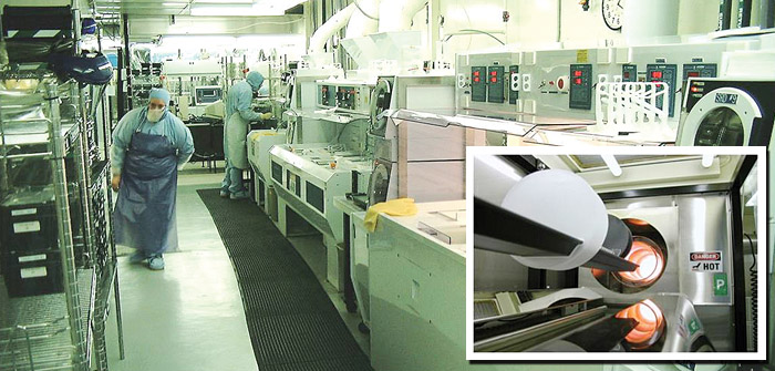
Most of that activity goes on in the fabrication area, which is innaccesible without a “bunny suit” and is unfortunately not nicknamed “The Fab Lab.” To get into the area, you must walk up a corridor past a wall of veritable scuba tanks attached to full face gas masks (in case of emergency), over a sticky mat designed to grab dirt from your shoes, and through a intermediate chamber, which operates both as an airlock and a dressing room, complete with lockers and rows of unused “bunny suits” on hangers.
On a wall outside the airlock room is a large plasma monitor, which displays humidity, temperature, air pressure and various other values around the fabrication area, all of which are controlled centrally. The values vary from zone to zone, to fit whatever task is being performed. Air pressure decreases the closer one gets to the boundaries of the fabrication area, which effectively works to push any meddlesome particulates or specks of dust out.
The laboratories are shrines of silvers and whites, tubes and plates, massive stainless boxes with tiny doors, bright lights which paint acetone scoured sinks in incandescent yellow, and smooth shining plates interrupted by the shadow of thick, solid bolts. The machinery itself is indecipherable and futuristic, yet grounded: the most impressive systems are connected to PC monitors which, despite showing rows of dense, inexplicable figures and microscopic renderings, wouldn’t look out of place in a nondescript office building, circa 2008. The perfect irony is that these hyper-advanced, unfathomably complicated machines would be completely useless without the very microprocessors they help to build.
This duality is a fitting representation of Microsemi itself, and the tech industry as a whole. According to Vandenberg, the scope of the semiconducter world was extremely concentrated. In the beginning, he says, all the majors companies were “in Silicon Valley.”
“Now,” he says, “it’s become truly a global business, and it’s extremely competitive.”
Therefore, Microsemi above all looks to “differentiate itself” from the competition. According to Vandenberg, this means constantly looking to innovate and develop new capabilities in an industry where being on the cutting edge is not a goal but a necessity. The production process is becoming increasingly automated, which may take the industry in new directions and have a radical effect on the way Microsemi positions itself within it.
It’s in this way that Microsemi, the microprocessor industry, and the very systems that drive them, run parallel to each other. Each builds upon itself: just as a machine running on silicon produces a thousand more, so too does the industry grow upon itself. In an age of rampant globalization, Microsemi looks to secure its niche by improving upon and evolving it’s products and practices, faster than any market could make it.
Microsemi
Location/Website: www.microsemi.com, 405 SW Columbia St., Bend, OR 97702
Phone: 541-382-8028
VP/General Manager Bend: Marc Vandenberg
No. Employees: 130
Year Established: 1984
Product/Service: Manufacturer of power semiconductors.
Outlook for Growth: A global business, Microsemi above all looks to “differentiate itself” from the competition.


